As engineers continue to make modern electronic devices smaller and smaller, materials scientists are exploring methods to construct these devices with increasing precision, a process known as nanofabrication. Ideally, this includes manipulating two-dimensional materials like graphene that offer unique properties not found in traditional materials.
Now, a team of researchers from the RIKEN Cluster for Pioneering Research and RIKEN Center for Advanced Photonics have developed a method to position optical quality carbon nanotubes (CNTs), one of the most intriguing and diverse 2D material components, in a precise way to take advantage of these unique properties.
“This technology has the potential to contribute to the development of atomically defined technologies that go beyond nanotechnology,” said team leader Yuichiro Kato in a press release announcing the breakthrough, “in which materials with precise structures at the atomic level are used as building blocks to design and build functions that are different from those of existing materials.”

Background: Why “Nanotubes” Are Essential
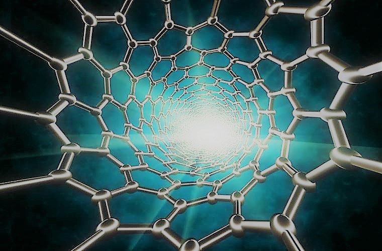
According to the team’s research published in the journal Nature Communications, carbon nanotubes are helpful in many applications, including LEDs, single-electron transistors, or even as a source of single photons for precision experimentation. Essentially tiny ‘tubes’ made up of graphene, CNTs can be twisted in specific ways, what some engineers call ‘magic angles,’ producing all kinds of effects not found in traditional materials.
The Debrief reported on this exact process, known as “twistronics,” last month, in which the University of California, Riverside Professor Nathan Gabor, one of the primary researchers on that project, told The Debrief, “I believe ‘twistronics’ will enable key outcomes to improve [things like] photovoltaics [and a whole range of technologies] because we can now manipulate materials in a highly precise way, essentially fine-tuning the placement of atoms in the crystal by twisting one layer relative to the other.”
However, according to the RIKEN press release, current methods of manipulating materials at this level involve the use of solvents or high-temperature treatments, which they say inevitably leaves the nanotubes dirty, hampering their optical characteristics. These limitations led researchers to examine what they termed ‘dry-transfer methods that don’t use solvents or other chemicals to manipulate the CNTs.
Analysis: Can We Build Nanotubes on the Atomic Scale?
After some initial study, the RIKEN team landed on anthracene, a chemical derived from oil, as a medium for moving and placing the CNTs with exacting precision. This is primarily because anthracene can be heated up and converted into a gas, or ‘sublimated,’ after the CNTs are put in place, leaving behind no material or material residue.
“Single-crystalline anthracene is used as a medium which readily sublimes by mild heating,” according to the published study, “leaving behind clean nanotubes and thus enabling bright photoluminescence.”
The team was able to pick up each nanotube on a scaffolding of anthracene, allowing them to place the CNT wherever they wanted. Once in place, the CNT is then heated, causing the anthracene to sublimate, or put more simply, turn from a liquid into a gas and simply float away. As the research team had hoped, once the anthracene had been removed, they were left with a pristine, perfectly placed CNT.
Further testing also revealed that the nanotube had not lost any of its optical or photoluminescent properties, a critical component in their ultimate usability. The paper also indicates that the team developed a method for monitoring the photoluminescence of the CNTs during the transfer process, “ensuring that a nanotube with the desired optical properties would be placed at a right location.”
Outlook: The Future Will Be Small…Very Small…
In the study’s conclusion, the team explains that the main advantages of their technique are not only precision placement and a clean transfer, but also the ability to manipulate the twist of the material, known as its ‘chirality,’ to take advantage of the unique twistronic properties of the CNTs.

As for how this technique may affect industrial and commercial applications, the research paper states that “efforts for further scaling will undoubtedly continue until we reach the ultimate limit where devices are constructed of components and interfaces with atomic precision: Atomically defined technology.”
This sentiment was echoed by Keigo Otsuka, the first author of the paper and a member of the RIKEN Cluster for Pioneering Research, who said, “We believe that this technology could contribute not only to the creation of nanodevices from carbon nanotubes with desired properties but also to the construction of higher-order systems that are based on the free combination of atomic layer materials and other nanostructures.”
Follow and connect with author Christopher Plain on Twitter: @plain_fiction
Don’t forget to follow us on Twitter, Facebook, and Instagram, to weigh in and share your thoughts. You can also get all the latest news and exciting feature content from The Debrief on Flipboard, and Pinterest. And subscribe to The Debrief YouTube Channel to check out all of The Debrief’s exciting original shows: DEBRIEFED: Digging Deeper with Cristina Gomez –Rebelliously Curious with Chrissy Newton